
THz Measurement Facility (THz Lab)

Theodore (Ted) Rappaport · Davood Shahrjerdi · Michael Knox · Hamed Rahmani

Focus: devices, circuits and radio channels above 100 GHz are poorly characterized, because test equipment at these frequencies is costly and usually set up for one kind of measurement. The THz Lab at NYU WIRELESS is a shared, multiuser facility that measures all three, from DC to 500 GHz.

  1. A shared facility from DC to 500 GHz
  2. Four-port probe stations
  3. SOLR calibration to 125 GHz on 28 nm CMOS
  4. Amplifier measurements from 140 to 220 GHz
  5. Open access and planned projects
  6. Spectrum and energy at 180, 220 and 280 GHz
  7. Channel sounder baseband in 65 nm CMOS
Sub-THz and THz measurementOn-wafer probingVNA calibrationRFIC characterizationChannel soundingShared facility
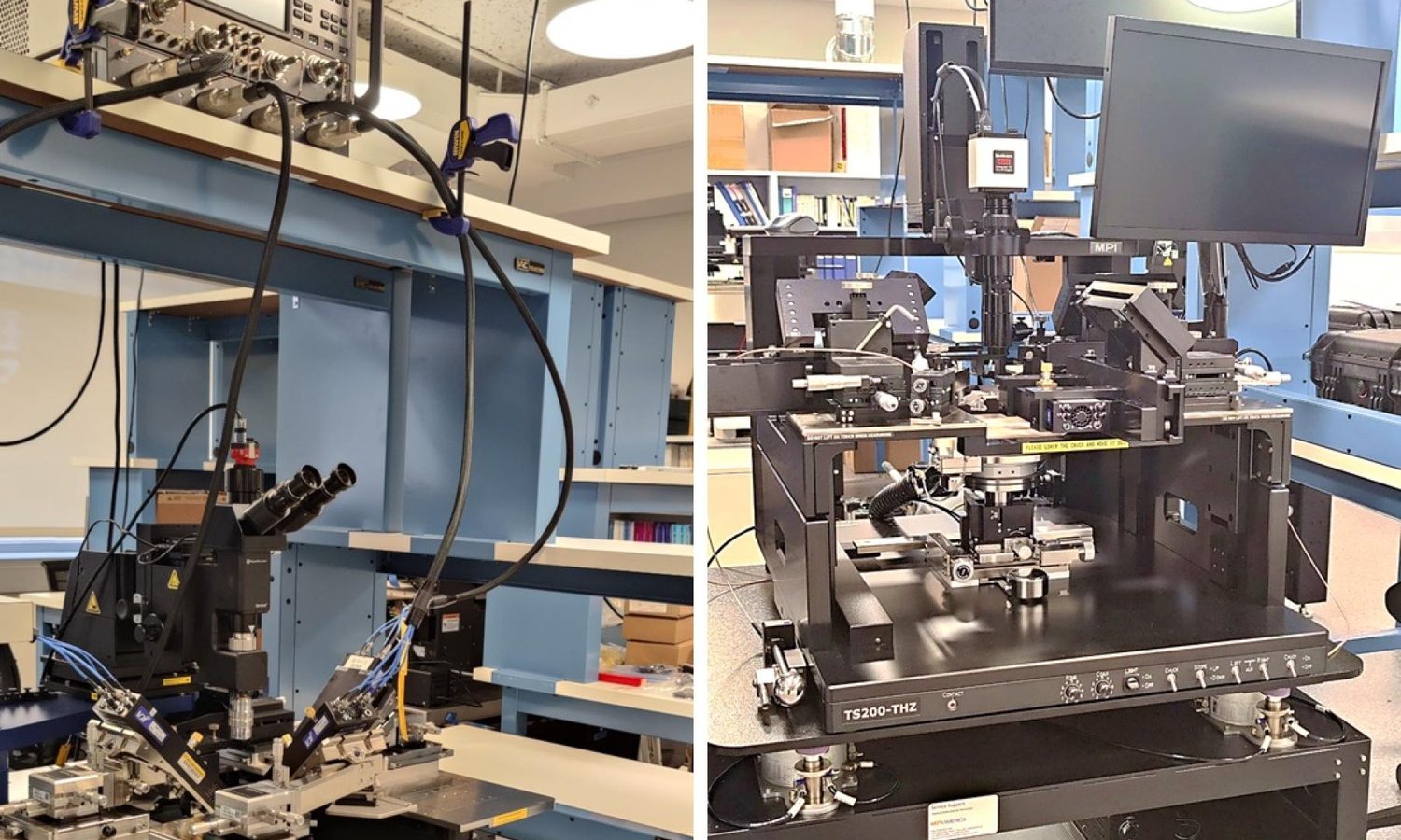
Two of the world's first four-port probe stations in the THz Lab: FormFactor with angled positioners (left) and MPI with flat positioners (right).
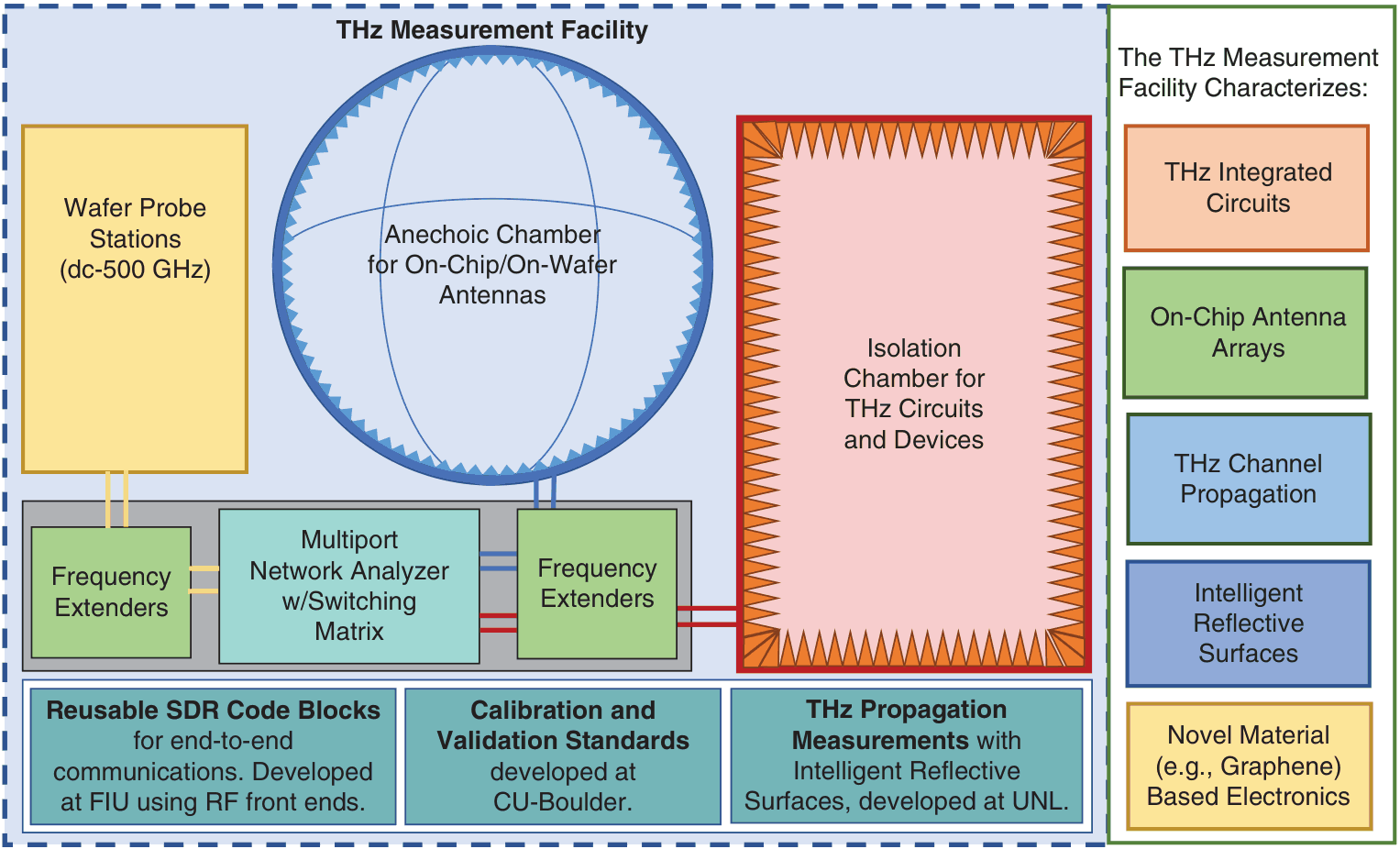
Facility concept proposed to NSF: one multiport network analyzer with frequency extenders and a switching matrix serves probe stations, an antenna chamber and an isolation chamber (Shakya et al., IEEE Microwave Magazine 2024).
A shared facility from DC to 500 GHz

Built with CU Boulder, Florida International University and the University of Nebraska–Lincoln under a US$3 million National Science Foundation (NSF) Major Research Instrumentation grant, the THz Lab supports radio-frequency integrated circuit (RFIC) measurements, radio propagation and metrology from DC to 500 GHz; its current radio-frequency (RF) inventory covers DC to 330 GHz (Shakya et al., IEEE Microwave Magazine 2024). A Keysight PNA-X network analyzer drives Virginia Diodes (VDI) frequency extenders in six waveguide bands, WR15 to WR2.2. In the concept proposed to NSF, a switching matrix shares the analyzer among probe stations and two chambers; the first build focuses on the probe stations.

Facility concept proposed to NSF: one multiport network analyzer with frequency extenders and a switching matrix serves probe stations, an antenna chamber and an isolation chamber (Shakya et al., IEEE Microwave Magazine 2024).
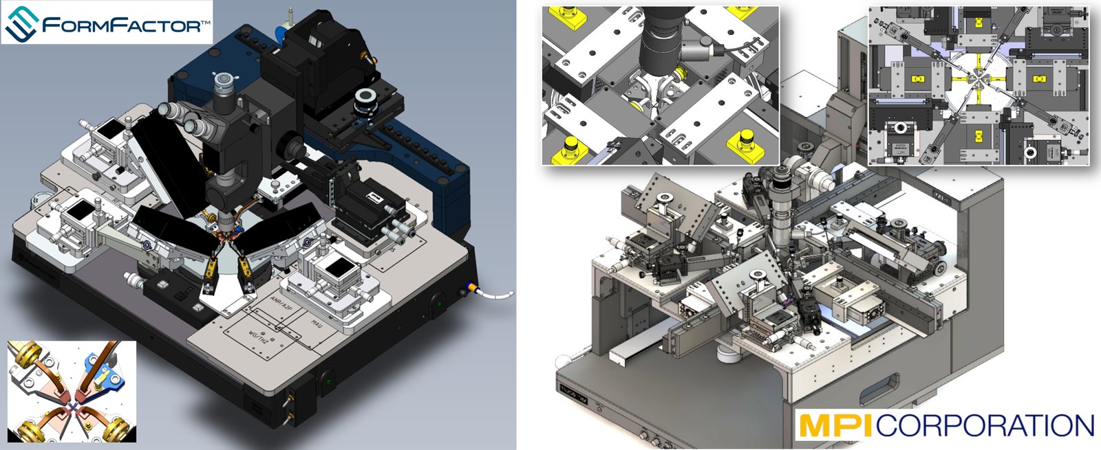
The FormFactor (left) and MPI (right) four-port probing designs, with probes landing from the East, West, North and South (Shakya et al., IEEE APMC 2025).

Four-port probe stations

Two of the first four-port probe stations in the world, designed independently for the lab by MPI Corporation and FormFactor, probe a die from all four sides at once, so multi-chain chips, couplers and quadrature mixers give full four-port S-parameters without repositioning probes (Shakya et al., IEEE APMC 2025). The FormFactor station uses 45° angled positioners on three sides and a flat North positioner. The MPI station, built on the 200 mm TS200-THZ, mounts any VDI extender directly on its probe in all four directions, with no S-bends.

The FormFactor (left) and MPI (right) four-port probing designs, with probes landing from the East, West, North and South (Shakya et al., IEEE APMC 2025).

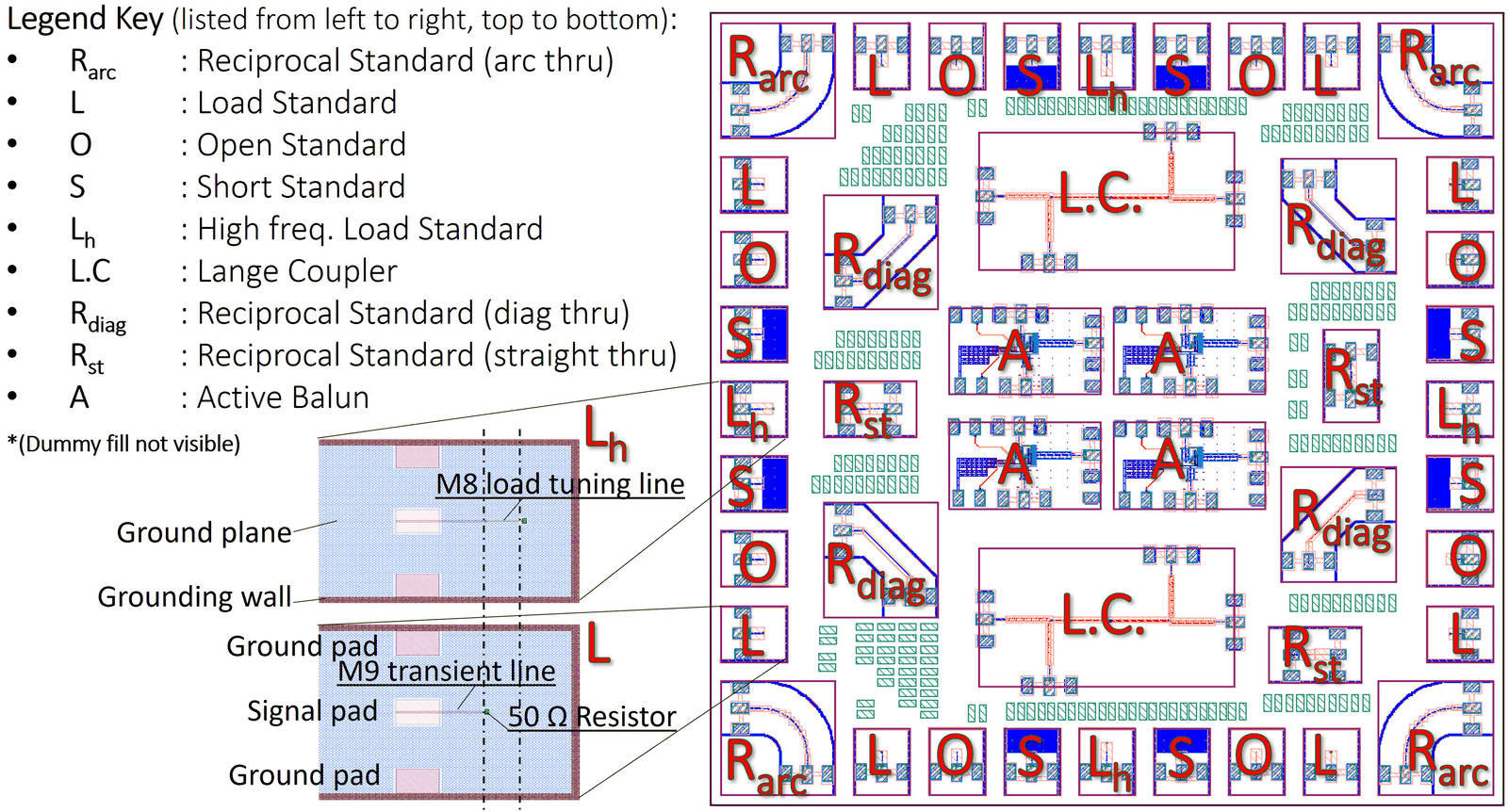
Layout of the 4 mm × 4 mm SOLR calibration chip in UMC 28 nm CMOS, with Short, Open and Load standards on each edge and reciprocal Thrus at the corners (Shakya et al., IEEE APMC 2025).

SOLR calibration to 125 GHz on 28 nm CMOS

Orthogonal probes cannot be joined by an ideal Thru, which rules out Short-Open-Load-Thru (SOLT) and Thru-Reflect-Line (TRL) calibration, and earlier on-wafer SOLR for orthogonal ports stayed below 26 GHz. The team taped out a 4 mm × 4 mm Short-Open-Load-Reciprocal (SOLR) standard set in UMC 28 nm complementary metal-oxide-semiconductor (CMOS) and characterized it with a virtual multiline TRL (Shakya et al., IEEE APMC 2025). HFSS simulations show valid calibration up to 125 GHz, with a corrected Thru loss below 1.5 dB.

Layout of the 4 mm × 4 mm SOLR calibration chip in UMC 28 nm CMOS, with Short, Open and Load standards on each edge and reciprocal Thrus at the corners (Shakya et al., IEEE APMC 2025).

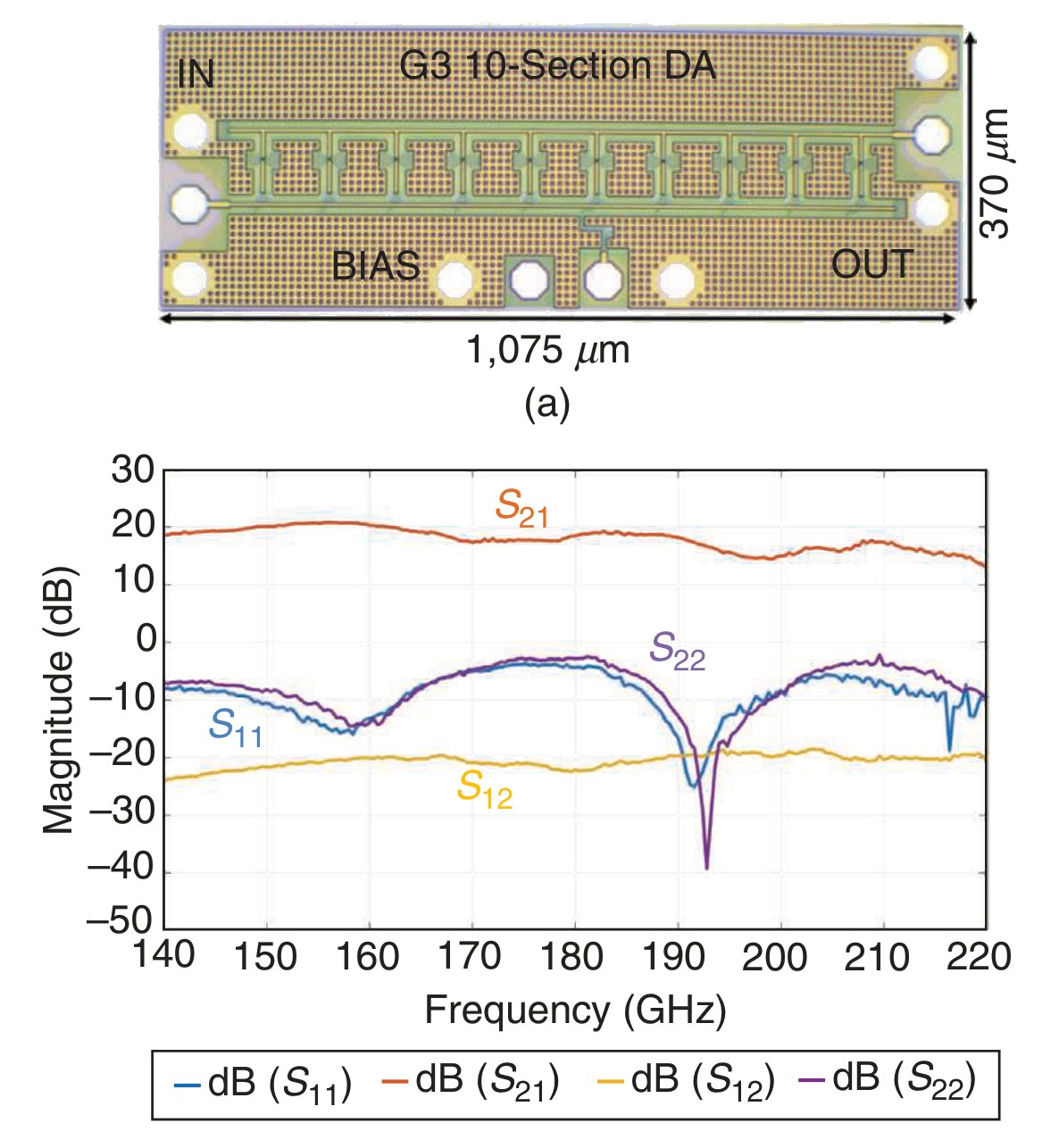
A Nokia Bell Labs SiGe distributed amplifier measured in the lab from 140 to 220 GHz, with peak gain over 18 dB (Shakya et al., IEEE Microwave Magazine 2024).
Amplifier measurements from 140 to 220 GHz

A ten-section Nokia Bell Labs distributed amplifier in 130 nm silicon-germanium (SiGe) BiCMOS was measured from 140 to 220 GHz, past the 170 GHz reached before, showing over 18 dB peak gain and a 1.4 THz gain-bandwidth product (Shakya et al., IEEE Microwave Magazine 2024). CU Boulder gallium nitride (GaN) monolithic microwave integrated circuits (MMICs), including a W-band power amplifier whose earlier large-signal tests did not reach saturation, are being re-evaluated. The lab also pursues free-space probing, where on-chip antennas replace fragile contact probes.
A Nokia Bell Labs SiGe distributed amplifier measured in the lab from 140 to 220 GHz, with peak gain over 18 dB (Shakya et al., IEEE Microwave Magazine 2024).
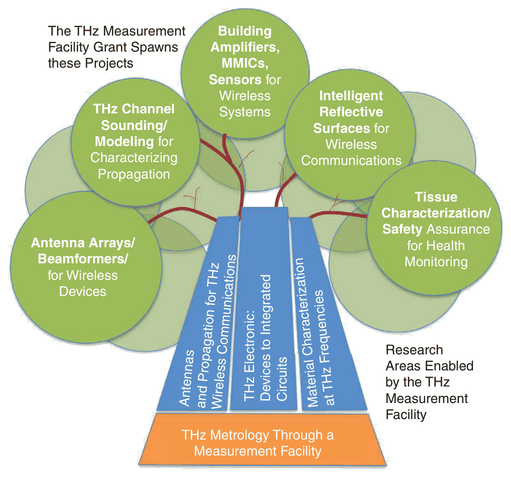
Research areas the facility supports, unified by THz metrology, and the projects they spawn (Shakya et al., IEEE Microwave Magazine 2024).

Open access and planned projects

Registered partners and collaborators get no-cost access, by visiting or by borrowing frequency extenders and converters as shippable channel-sounder front ends; borrowers pay shipping and insurance, and access follows U.S. export controls. CU Boulder contributes metrology and calibration standards, FIU a 140 GHz software-defined radio baseband, and UNL rural propagation and reconfigurable intelligent surface (RIS) work. Planned projects include 3D-printed RIS for 100–500 GHz, radio-astronomy array coupling studies, a multipixel graphene THz receiver and RF safety studies. Details are on the THz Lab website.

Research areas the facility supports, unified by THz metrology, and the projects they spawn (Shakya et al., IEEE Microwave Magazine 2024).

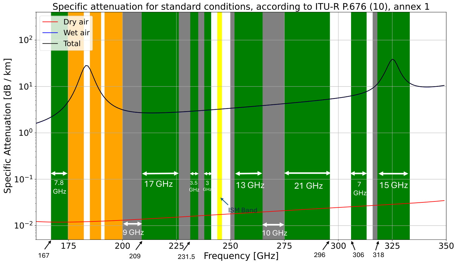
ITU allocations from 170 to 350 GHz over atmospheric attenuation, showing the 183 GHz absorption peak and contiguous bands of up to 21 GHz (Rappaport, Humphreys & Nie, npj Wireless Technology 2025).

Spectrum and energy at 180, 220 and 280 GHz

A survey of ITU, FCC and ETSI rules identifies candidate 6G bands above 100 GHz: a 180 GHz short-range band with 7.8 GHz of spectrum, 209–225 GHz with 17 GHz contiguous, and 275–296 GHz with 21 GHz not yet allocated. Higher bands can also save energy: over 100 m, a 140 GHz link with 4 GHz of bandwidth delivers 2.18 Gb/J against 0.99 Gb/J for a 28 GHz, 400 MHz link (Kanhere et al., IEEE Wireless Communications 2022). NYU WIRELESS campaigns planned next target 3.7, 180, 220 and 285 GHz.

ITU allocations from 170 to 350 GHz over atmospheric attenuation, showing the 183 GHz absorption peak and contiguous bands of up to 21 GHz (Rappaport, Humphreys & Nie, npj Wireless Technology 2025).

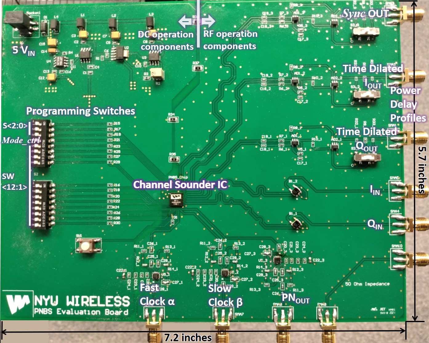
The 7.2 × 5.7 inch evaluation board with the 65 nm CMOS channel sounder IC at its center (Shakya et al., IEEE TCAS-II 2021).

Channel sounder baseband in 65 nm CMOS

Earlier NYU WIRELESS work put the sliding-correlator baseband on a 65 nm CMOS chip, the first gigabit-per-second channel-sounder baseband in low-cost CMOS, with 2 GHz RF bandwidth and 1 ns multipath resolution (Shakya, Wu & Rappaport, IEEE GLOBECOM 2020). In the 142 GHz sounder, its evaluation board replaced the PXIe baseband chassis, cutting weight by over 40 lb and volume from 18×18×8 in to 7.2×5.7×0.1 in (Shakya et al., IEEE TCAS-II 2021).

The 7.2 × 5.7 inch evaluation board with the 65 nm CMOS channel sounder IC at its center (Shakya et al., IEEE TCAS-II 2021).

Faculty

Theodore (Ted) RappaportDavood ShahrjerdiMichael KnoxHamed Rahmani

Students

Dipankar ShakyaEthan ShiehMingjun Ying